N Type , InP(Indium Phosphide) Substrate,3”, Prime Grade -Compound
Semiconductor
PAM-XIAMEN offers InP wafer – Indium Phosphide which are grown by
LEC(Liquid Encapsulated Czochralski) or VGF(Vertical Gradient
Freeze) as epi-ready or mechanical grade with n type, p type or
semi-insulating in different orientation(111)or(100).
Indium phosphide (InP) is a binary semiconductor composed of indium
and phosphorus. It has a face-centered cubic (“zinc blende”)
crystal structure, identical to that of GaAs and most of the III-V
semiconductors.Indium phosphide can be prepared from the reaction
of white phosphorus and indium iodide[clarification needed] at 400
°C.,[5] also by direct combination of the purified elements at high
temperature and pressure, or by thermal decomposition of a mixture
of a trialkyl indium compound and phosphide. InP is used in
high-power and high-frequency electronics[citation needed] because
of its superior electron velocity with respect to the more common
semiconductors silicon and gallium arsenide.
N Type, InP Substrate, 3”, Prime Grade
| 3"InP Wafer Specification | | | |
| Item | Specifications |
| Conduction Type | N-type | N-type |
| Dopant | Undoped | Sulphur |
| Wafer Diameter | 3" |
| Wafer Orientation | 100±0.5° |
| Wafer Thickness | 600±25um |
| Primary Flat Length | 16±2mm |
| Secondary Flat Length | 8±1mm |
| Carrier Concentration | ≤3x1016cm-3 | (0.8-6)x1018cm-3 | (0.6-6)x1018cm-3 | N/A |
| Mobility | (3.5-4)x103cm2/V.s | (1.5-3.5)x103cm2/V.s | 50-70cm2/V.s | >1000cm2/V.s |
| Resistivity | N/A | N/A | N/A | >0.5x10⁷Ω.cm |
| EPD | <1000cm-2 | <500cm-2 | <1x103cm-2 | <5x103cm-2 |
| TTV | <12um |
| BOW | <12um |
| WARP | <15um |
| Laser Marking | upon request |
| Suface Finish | P/E, P/P |
| Epi Ready | yes |
| Package | Single wafer container or cassette |
What is a Test Wafer?
Most test wafers are wafers which have fallen out of prime
specifications. Test wafers may be used to run marathons, test
equipment and for high-end R & D. They are often a cost-effective
alternative to prime wafers.
 | Electron Hall mobility versus temperature for different doping
levels.
Bottom curve - no=Nd-Na=8·1017 cm-3;
Middle curve - no=2·1015 cm-3;
Top curve - no=3·1013 cm-3.
(Razeghi et al. [1988]) and (Walukiewicz et al [1980]). |
 | Electron Hall mobility versus temperature (high temperatures):
Bottom curve - no=Nd-Na~3·1017 cm-3;
Middle curve - no~1.5·1016 cm-3;
Top curve - no~3·1015 cm-3.
(Galavanov and Siukaev[1970]). |
For weakly doped n-InP at temperatures close to 300 K electron
drift mobility:
µn = (4.2÷5.4)·103·(300/T) (cm2V-1 s-1)
 | Hall mobility versus electron concentration for different
compensation ratios.
θ = Na/Nd, 77 K.
Dashed curves are theoretical calculations: 1. θ = 0; 2. θ = 0.2;
3. θ = 0.4; 4. θ = 0.6; 5. θ = 0.8;
(Walukiewicz et al. [1980]).
Solid line is mean observed values (Anderson et al. [1985]). |
 | Hall mobility versus electron concentration for different
compensation ratios
θ =Na/Nd, 300 K.
Dashed curves are theoretical calculations: 1. θ = 0; 2. θ = 0.2;
3. θ = 0.4; 4. θ = 0.6; 5. θ = 0.8;
(Walukiewicz et al. [1980]).
Solid line is mean observed values (Anderson et al. [1985]). |
Approximate formula for electron Hall mobility
µ=µOH/[1+(Nd/107)1/2],
where µOH=5000 cm2V-1 s-1,
Nd- in cm-3 (Hilsum [1974])
At 300 K, the electron Hall factor rn≈1 in n-InP.
for Nd > 1015 cm-3.
 | Hole Hall mobility versus temperature for different doping (Zn)
levels.
Hole concentration at 300 K: 1. 1.75·1018 cm-3; 2. 3.6·1017 cm-3;
3. 4.4·1016 cm-3.
θ=Na/Nd~0.1.
(Kohanyuk et al. [1988]). |
For weakly doped p-InP at temperature close to 300 K the Hall
mobility
µpH~150·(300/T)2.2 (cm2V-1 s-1).
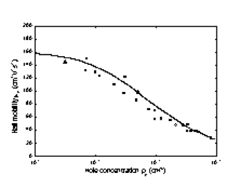 | Hole Hall mobility versus hole density, 300 K (Wiley [1975]).
The approximate formula for hole Hall mobility:
µp=µpo/[1 + (Na/2·1017)1/2], where µpo~150 cm2V-1 s-1, Na- in cm-3 |
At 300 K, the hole factor in pure p-InP: rp~1
Optoelectronic Applications
InP based lasers and LEDs can emit light in the very broad range of
1200 nm up to 12 µm. This light is used for fibre based Telecom and
Datacom applications in all areas of the digitalised world. Light
is also used for sensing applications. On one hand there are
spectroscopic applications, where a certain wavelength is needed to
interact with matter to detect highly diluted gases for example.
Optoelectronic terahertz is used in ultra-sensitive spectroscopic
analysers, thickness measurements of polymers and for the detection
of multilayer coatings in the automotive industry. On the other
hand there is a huge benefit of specific InP lasers because they
are eye safe. The radiation is absorbed in the vitreous body of the
human eye and cannot harm the retina. InP lasers in LiDAR (Light
Detection And Ranging) will be a key component for the mobility of
the future and the automation industry.
Are You Looking for an InP Wafer?
PAM-XIAMEN is your go-to place for everything wafers, including InP
wafers, as we have been doing it for almost 30 years! Enquire us
today to learn more about the wafers that we offer and how we can
help you with your next project. Our group team is looking forward
to providing both quality products and excellent service for you!

 Substrate,3”, Prime Grade -Compound Semiconductor on sale")
 Substrate,3”, Prime Grade -Compound Semiconductor on sale")


 Crystal Wafer , 3”, Dummy Grade for sale")
